AMD To Develop Semi-Custom Graphics Chip For Intel
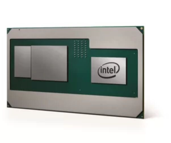
In an interesting turn of events, AMD announced that it’s creating a semi-custom GPU for a forthcoming Intel Multi-Chip Package (MCP).
AMD’s GPU will snap into an eighth-generation Intel processor that utilizes HBM2 memory, a first for a mobile PC, and Intel’s EMIB interconnect. Both Intel and AMD confirmed development of the new H-Series processors, which also marks the first use of EMIB technology in a consumer product.
There have been rumors, beginning with a forum post earlier this year by HardOCP’s Kyle Bennet, that claimed AMD is developing GPUs for Intel. This led to quite the industry buzz, and a short-term stock gain for AMD, but it was largely dismissed as an unfounded rumor. At the time, Intel also issued an official statement claiming that it had not licensed AMD’s graphics technology. But more recently AMD has mentioned a big semi-custom chip win in several of its latest financial earnings calls, but declined to name the new customer. It appears to be Intel.
AMD finally released an official statement this morning:
“Our collaboration with Intel expands the installed base for AMD Radeon GPUs and brings to market a differentiated solution for high-performance graphics,” said Scott Herkelman, vice president and general manager, AMD Radeon Technologies Group. “Together, we are offering gamers and content creators the opportunity to have a thinner-and-lighter PC capable of delivering discrete performance-tier graphics experiences in AAA games and content creation applications. This new semi-custom GPU puts the performance and capabilities of Radeon graphics into the hands of an expanded set of enthusiasts who want the best visual experience possible.”
The Wall Street Journal claims the new chip will not compete with AMD’s forthcoming Ryzen Mobile processors. AMD hasn’t officially confirmed the information, but it seems to be true, given the few details Intel has released about the H-Series design. Intel’s H-Series also falls into the 35-45W TDP envelope, while the Ryzen Mobile processors are 15W processors.
Intel also released a statement:
The new product, which will be part of our 8th Gen Intel Core family, brings together our high-performing Intel Core H-series processor, second generation High Bandwidth Memory (HBM2) and a custom-to-Intel third-party discrete graphics chip from AMD’s Radeon Technologies Group* – all in a single processor package.
Notably, Intel’s eighth-generation lineup consists of three separate nodes/architectures: the 14nm+ Kaby Lake-R (refresh), 14nm++ Coffee Lake, and 10nm Cannon Lake. Intel hasn’t disclosed which process it will employ with the new processor, but it is likely paired with the forthcoming 10nm Cannon Lake processors that have long been scheduled for release early next year. It’s also logical to assume the AMD GPU employs Vega cores, especially given the use of HBM2 and the unique power delivery system (covered below).
Intel has traditionally used Nvidia IP for its graphics solutions through a patent-sharing license, but that agreement expired earlier this year. The agreement allows Intel to use Nvidia’s IP in perpetuity, but it only applies to the IP shared during the licensing period. That means Intel doesn’t have access to newer Nvidia IP. Intel confirmed to us that its new arrangement with AMD doesn’t include licensing of AMD’s technology; instead, Intel is merely purchasing finished semi-custom products from AMD that it fabs with its partners. That means Intel likely isn’t abandoning its own internal GPU development programs. Intel also confirmed to us that it approached AMD to begin the project.
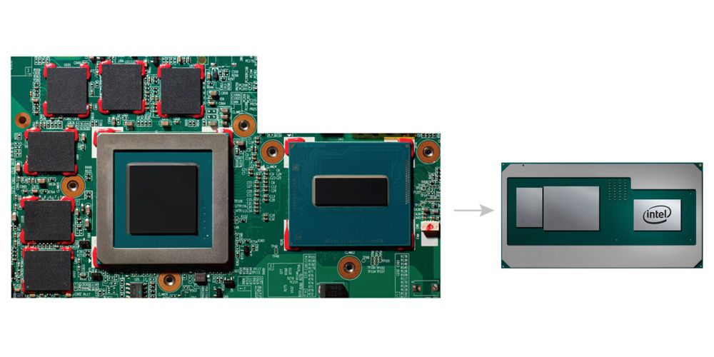
Intel claims the new design will allow for thinner and lighter devices, such as notebooks, 2-in-1s, and mini-desktops, by combining all of the components into one device. Intel claims the new processor, which obviously will power high-end mobile products, reduces the component footprint by half compared to existing motherboards. That equates to a real estate savings of 1,900mm2. That enables OEMs to make thinner and lighter devices while also bulking up the thermal solution. Increased thermal dissipation is a key enabler for high-power mobile devices because it allows the device to operate at a higher level of performance for a longer duration.
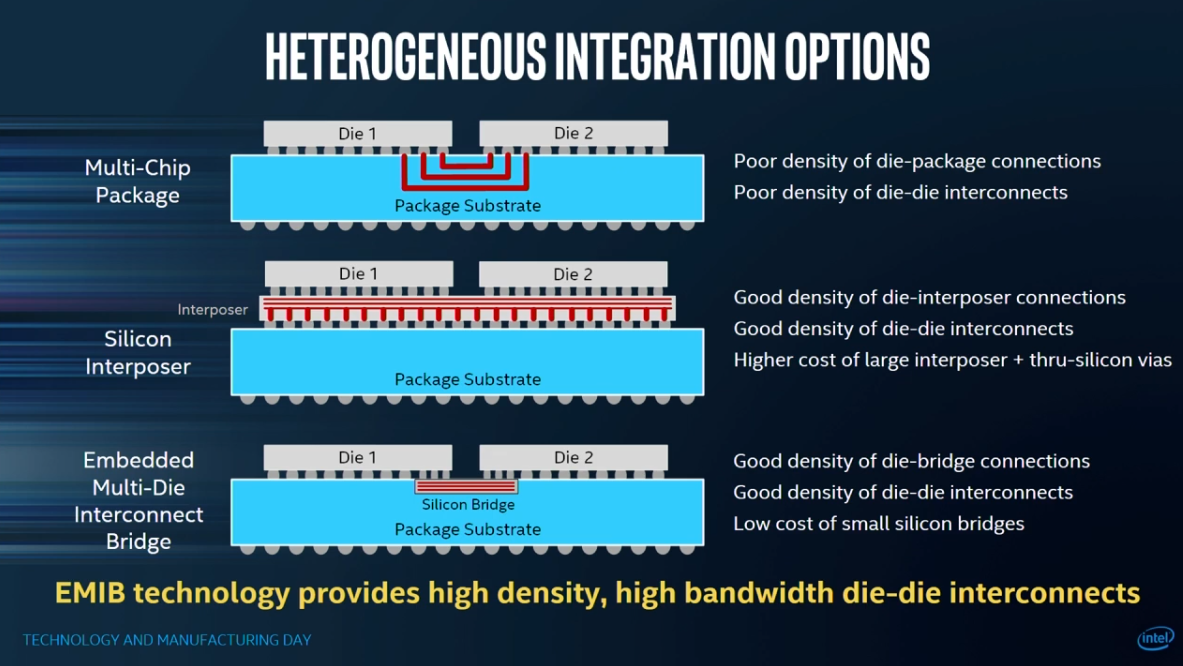
Intel gave us the details of its new EMIB (Embedded Multi-Die Interconnect Bridge) earlier this year at the Hot Chips conference. Our Hot Chips 2017: Intel Deep Dives Into EMIB article covers all of the details of the new technology. In a nutshell, EMIB is an interconnect that ties multiple discrete chips together into a single heterogeneous package. The connection consists of a small silicon bridge, or several of them, embedded into the package substrate.

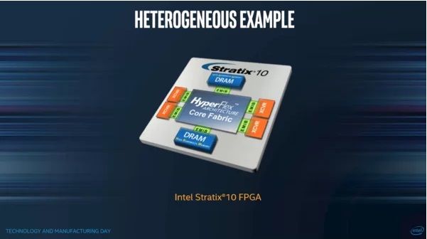
Intel designed the technology to tie its chips together with “chiplets,” which are small, re-usable, third-party IP building blocks that can be processors, transceivers, memory, GPUs, or other types of components. Intel can mix and match the chiplets, much like Lego blocks, and connect them to its processors to create custom designs for different applications. Above, we see Intel’s plans for matching its Stratix FPGAs with several chiplets, but in the case of the new eighth-gen processors, the components will consist of AMD’s GPU and several HBM2 packages.
The different components communicate over a quasi-standardized communication protocol, which should allow vendors to protect key portions of their IP.
Intel added its own software drivers to the H-Series processor to manage temperature, power delivery, and performance in real time. This new software allows the processor to dynamically adjust the power delivery ratio between the processor and the GPU based upon the workload, much like AMD’s new power delivery subsystem in its Ryzen Mobile products. That will help reduce overall power consumption. HBM2 also offers more performance and lower power consumption than GDDR5 memory, while also consuming less precious real estate.
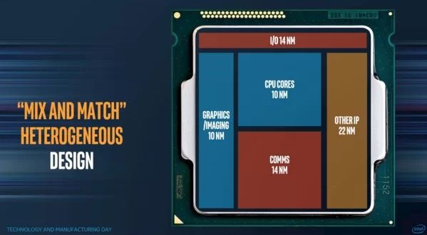
The dawn of the chiplet marks a tremendous shift in the semiconductor industry. The industry is somewhat skeptical of the chiplet concept, largely because it requires competitors to arm their competition, but the Intel and AMD collaboration proves that it can work with two of the biggest heavyweights in the computing industry. Not to mention bitter rivals. Industry watchers have also largely been in agreement that EMIB would not filter down to the consumer market for several years, but the announcement clearly proves the technology is ready for prime time.
DARPA initially brought the chiplet revolution to the forefront with its CHIPS (Common Heterogeneous Integration and Intellectual Property (IP) Reuse Strategies) initiative, which aims to circumvent the limitations of the waning Moore’s Law.
Intel plans to bring the new devices to market early in 2018 through several major OEMs. Neither Intel nor AMD have released any detailed information, such as graphics or compute capabilities, TDP ratings, or HBM2 capacity, but we expect those details to come to light early next year.