
Intel Debuts Meteor Lake Die, ‘Intel 4’ Node: 20% Higher Clocks at Same Power, 2X Area Scaling
Intel announced the first details of its ‘Intel 4’ process node and shared an image of a Meteor Lake compute die at the 2022 IEEE VLSI Symposium. Intel claims impressive results with its new ‘Intel 4’ node over its previous-gen ‘Intel 7’ node, including 21.5% higher frequencies at the same power, or a 40% power reduction at the same frequency. Intel also claims a 2X area scaling improvement, meaning it has doubled transistor density for the high-performance libraries. The Intel 4 node is also the company’s first to use EUV lithography. That’s just to name a few among many other notable advancements that we’ll cover in more detail below.
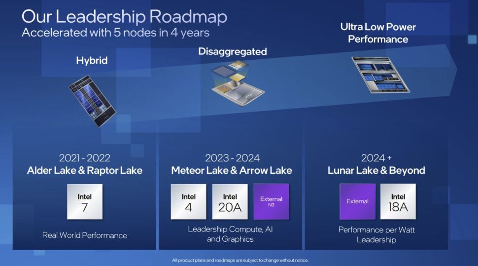
Intel’s missteps with the 10nm process saw it lose its process tech leadership to TSMC, not to mention cede performance leadership to AMD in the CPU market. As such, all eyes are on the company as its ‘Intel 4’ process, which we’ll refer to as ‘I4,’ comes to market in 2023.
Intel tried to scale too aggressively with its 10nm node to reach a 2.7X scaling goal. That led to constant delays due to the simultaneous incorporation of multiple new technologies, some of which obviously didn’t meet development targets. For I4 and beyond, intel is taking a more modular approach and introducing newer technologies step by step as it progresses to each node, thus delivering a more gradual cadence that it hopes will avoid the delays we’ve seen in the past.
Intel is developing multiple nodes in parallel to deliver on its promise of five nodes in four years, and I4 is the second step in that journey. First, let’s take a closer look at the Meteor Lake die, then dive into the details of the I4 presentation.
Intel Meteor Lake Die Shot
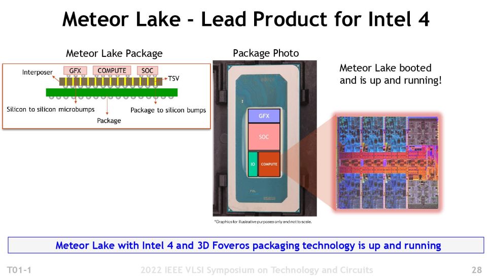
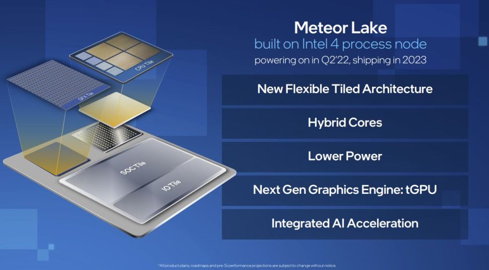
Intel’s Meteor Lake will be the first product to market with the I4 process. Intel powered on the compute silicon in April 2022 and claims it has already booted several operating systems. Intel says Meteor Lake is on track for a 2023 launch.
Meteor Lake will use Intel’s Foveros 3D packaging tech, just as we saw with the Lakefield processors. However, this will be Intel’s first foray into high-volume manufacturing with this leading-edge packaging tech.
Intel will connect the four die (called ’tiles’ in Intel parlance) to an interposer through TSV connections. Intel hasn’t disclosed if this interposer will be active or passive or if it will hold caches or other control circuitry. Intel will mount four tiles atop this interposer: the compute tile, I/O tile, SOC tile, and graphics tile.
Intel has specified that compute tile will use I4 but hasn’t said which nodes it will use for the other tiles. During its Analyst Day earlier this year, the company shared the slide in the above album that lists TSMC’s N3 (3nm) node with the Meteor and Arrow Lake processors. This is largely thought to comprise the graphics tile.
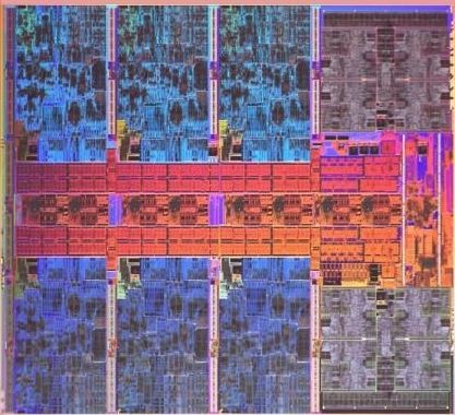
As with Alder Lake, the Meteor Lake chips have an x86 hybrid architecture. In this case, we have six p-cores and eight e-cores. The exploded view of the compute die shows us six blue-colored Redwood Cove performance cores (p-cores), used for latency- and performance-sensitive work. We also see two four-core clusters of Crestmont efficiency cores (e-cores) in purple. These cores step in for background and multi-threaded tasks. The center of the chip contains the L3 caches and interconnect circuitry. Intel has yet to provide a further description of the differences between the SoC and I/O tiles, with the former a likely candidate for memory controllers and PCIe interfaces, while the latter could be for Thunderbolt and other PCH-types of interfaces.
Intel isn’t giving us much to work with here, but the company shared far more expansive details on the I4 process node that makes the compute die tick.
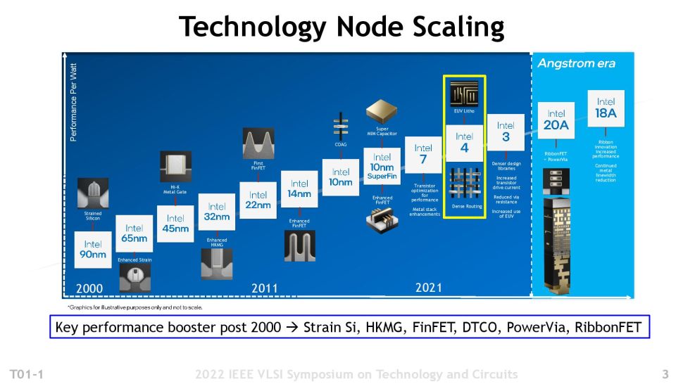
As a quick reminder, Intel recently renamed its process nodes to have a more uniform naming convention that aligns with its primary competitors (third-party foundries TSMC and Samsung). Intel’s current flagship process node, Intel 7, used to be called 10nm. Additionally, the I4 node used to be referred to as 7nm. We’ll stick with the current naming scheme so there’s no (or at least less) confusion.
Intel, like its competitors, usually bakes two versions of each process node — a high-density library that looks to squeeze in the most transistors possible at the expense of performance, and a high-performance library that trades off some transistor density to provide more performance. Naturally, Intel and its competitors always refer to the high-density library for the density metrics they use for marketing. Still, most of the flagship high-performance chips you see on the market actually use the less-dense library.
Quite surprisingly, Intel isn’t creating a high-density library for its I4 node; instead, it will focus solely on high-performance products for I4. Intel says that I4’s successor, ‘Intel 3,’ will come with both high-performance and high-density libraries. Notably, Intel recently announced that it would delay its Granite Rapids Xeons from 2023 to 2024 due to switching the design from I4 to ‘Intel 3’ (I3).
The I4 node is forward compatible with I3, so designs can be moved between the two without going through the usual time-consuming steps of porting an architecture. The I3 process will also have enhanced transistors and interconnects, along with more EUV layers to further simplify the design. The I3 node will be 18% faster than I4 and will be the first new node Intel will offer its customers through Intel Foundry Services (IFS) (the company already offers its existing 16nm).
After I3, Intel will move to the angstrom era with the 20A and 18A nodes, both of which will introduce even more exotic new tech, like new RibbonFETs (gate all around/nanosheet) and PowerVia (backside power delivery) tech.